What is NAND Flash Memory?
NAND flash is a common type of non-volatile memory (NVM). Unlike a volatile memory type, such as DRAM, NAND flash retains data when power is removed and so has many applications.
But what is NAND memory and how does it work?
IN THIS GUIDE:
In this guide we will explore:
Though the focus of this guide is on NAND memory we will compare the memory type against NOR on several occasions.
What does NAND mean?
The term comes from the logic expression Not AND, whereas NOR is Not OR. Both functions can be created in electronic circuitry using transistors (acting like switches) in either a series configuration for NAND or in parallel for NOR.
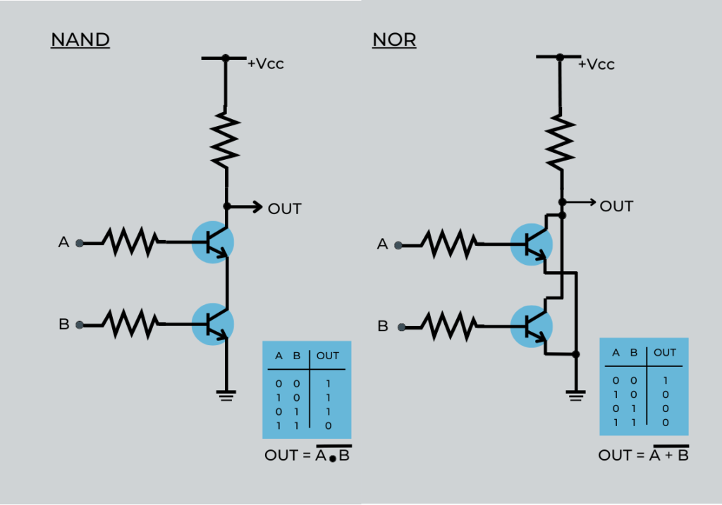
Above, the circuits, truth tables and Boolean expressions for NAND (on the left) and NOR functions.
Whilst not present to act as traditional switches in memory, the respective configurations are at the heart of NAND and NOR flash. Each transistor is effectively present to store data (one bit or more, see later). Also, we tend to talk in terms of NAND and NOR cells rather than gates or transistors.
NAND flash cells
A flash cell is effectively an N-channel MOSFET transistor with an extra gate – called the floating gate – which is sandwiched between two insulators. Probably the opposite of what you might expect, when charged the floating gate represents a logic 0 and is considered programmed. Uncharged the cell is erased and represents a logic 1.
Let’s discuss how to write, read and erase data
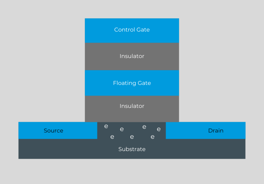
To charge the floating gate, a high voltage is applied to the control gate, while the drain and source are grounded. Electrons move from the silicon substrate (see above diagram) through an effect known as Fowler-Nordheim tunnelling. There the charge remains even when the control gate voltage is removed, which is core to the memory’s non-volatile behaviour.
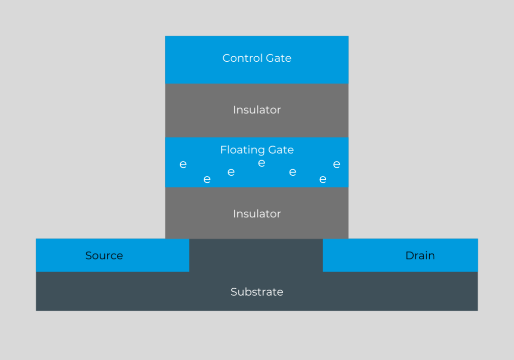
To erase the cell, a positive voltage is applied to the silicon substrate. This causes the electrons to tunnel back through the lower insulator (in the above diagram) and the floating gate is no longer charged.
Reading the memory cell is a case of determining if the floating gate is charged or not. To do this, the process is similar to the way in which a standard transistor can be used as a switch. A known voltage is applied to the control gate (along the ‘word line’ in NAND, see later). A voltage is also applied to the drain (this connection is along the ‘bit line’ in NAND, see later) and the drain current flow is compared to a threshold. If the drain current is above the threshold, this means the potential applied to the control gate was enough to turn on the transistor.
Because we are talking in terms of charge (an analogue quantity), there is a degree of uncertainty – where it is hard to say whether it is definitely representing a 1 or definitely representing a 0. However, it is this analogue behaviour that allows a single cell to represent more than a single bit of data – see later.
NAND flash cells are connected in series (daisy-chained, drain to source). The first cell’s drain is connected to the bit line via a standard (i.e., not floating gate) transistor, as is the last cell’s source to the source line. NOR flash cells are connected in parallel, with every cell’s drain connected to the bit line and the source connected to the source line. The following two diagrams show the differences.
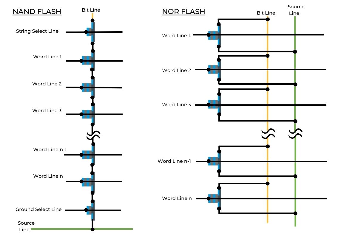
Above, the series (for NAND) and parallel (for NOR) connectivity between cells is shown.
There are pros and cons associated with both connection schemes. For example, the series connection in NAND reduces the number of ground wires and bit lines – making it a very compact memory type (i.e., less chip real estate and therefore lower cost) but we do not have direct access to individual cells, which slows down memory access and increases wear.
By contrast, in NOR, the transistors are in parallel so every drain connects to the bit line and every source to the source line, which is how individual cells can be accessed. This makes for faster access, but more silicon real estate is required which increases cost.
As a memory cell (i.e., irrespective of whether it is in NAND or NOR flash) it is good for between 50,000 and 100,000 program/erase cycles – both of which are ‘harder’ on the cell (than reading) because of the high voltage used. The transistors degrade and the floating gates take longer to charge and discharge. As mentioned, NAND will wear quicker than NOR because of lack of direct access to individual cells However, when embedded in a memory device (be it an SSD or a portable/removable card or drive), wear levelling circuitry is present.
NAND versus NOR
Here are the main differences between NAND and NOR.
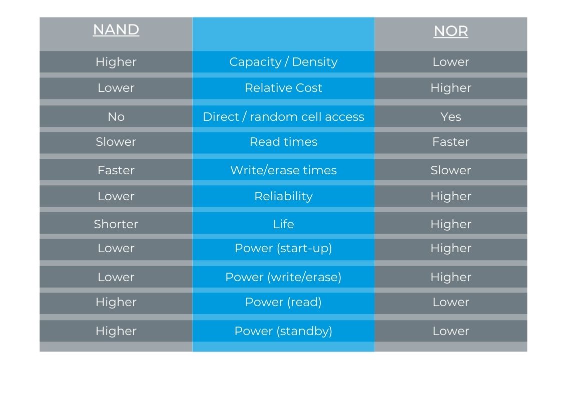
In general, NAND tends to be used for data storage, particularly in low-cost consumer goods (but there are many other applications – again, see our What is NAND Memory Used For? guide). NOR on the other hand tends to be used for program/code storage and execution.
However, as the above table illustrates, there are more factors than just capacity, cost and speed to consider when selecting a memory type. For example, if the memory is to be incorporated into a battery-power product, the power consumed during start-up, write, erase and read (and while on standby) must be factored in; and all of those will be driven by the product’s features and anticipated levels of use.
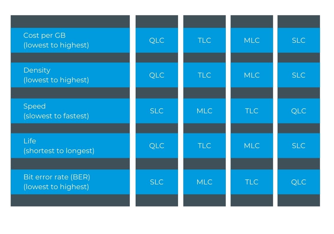
Bits per NAND cell
Above we explained how a floating gate transistor can be used to store one bit of data. This would be a single level cell (SLC). As mentioned, the data is represented as a charge (an analogue quantity) that is compared against a reference voltage to determine if the charge represents a 1 or a 0.
By comparing the charge to more than a single reference voltage the cell can be used to represent more than a single bit of data. Specifically, if:
- Three reference voltages are used, the cell can be considered to have four possible states. Expressed as two bit binary numbers these are 00, 01, 10 and 11. The technique is called dual or multilevel cell (DLC or MLC).
- The use of seven reference voltages allows for the representation of eight three-bit numbers (000 to 111) and is termed triple-level cell (TLC).
- The use of 15 reference voltages allows for the representation of 16 four-bit numbers (0000 to 1111) and is termed quad-level cell (QLC).
The main benefits are higher density/capacity memory. There are trade-offs though, as the following table shows.
NAND flash memory architecture
A NAND flash memory die contains planes, and planes hold blocks. A block is effectively an array (or matrix) of strings (highlighted below as a column) and pages (rows of cells).
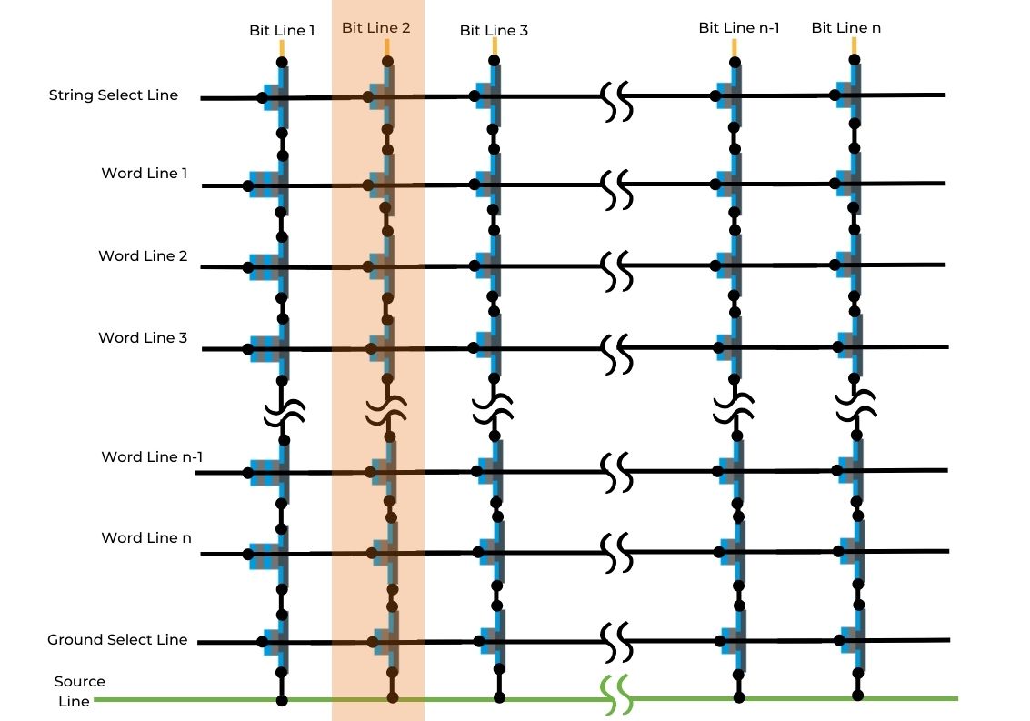
Above, a string is series of memory cells. The string for Bit Line is highlighted.
A string is the smallest volume that can be read and is typically 32 or 64 cells long. A page is several thousand cells that share the same word line. Page size is typically 64 or 128K.
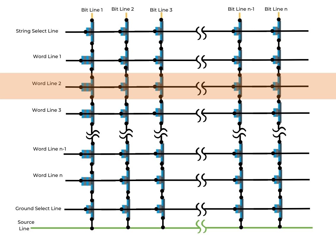
Above, a NAND page is a row of cells. The page for Word Line 2 is highlighted.
A 2GB NAND device will have 2048 blocks, with 64 pages per block. Each page will have 2048 bytes reserved for data storage plus 64 bytes reserved for error correction and wear levelling, for example.
3D NAND
Above we discussed and illustrated NAND flash memory architecture, in terms of electrical / cell connectivity. We also discussed the advantages (and illustrated the trade-offs) of representing more than one data bit in a NAND cell: MLC, TLC or QLC.
When fabricating NAND cells on a silicon wafer there two ways of laying them out, in a plane (2D) or stacked (3D).
Compared to 2D NAND, 3D NAND:
- Accommodates more write cycles (so less wear)
- Requires less power
- Requires less space
- Is cheaper
…whether we’re talking SLC, MLC, TLC or QLC.
There’s no real ‘2D versus 3D’ argument, as the latter technology is an obvious choice when designing memory into a product. Also, if the 2D NAND memory in a product is nearing the end of its life, upgrading to 3D NAND is a practical solution – noting that the 2D NAND need not be wasted, it can still be used as an SSD for long-term storage (read only backups).
Interfacing with NAND flash memory
Most flash memory uses the Common Flash Memory Interface (CFI), an open standard jointly developed by AMD, Intel, Sharp and Fujitsu, and approved by the non-volatile-memory subcommittee of the Joint Electron Device Engineering Council (JEDEC).
Flash memory compliant with the standard contains information about its capacity, configuration and voltage and timing.
JEDEC’s JESD68.01 can be download here (registration or login is required).